Capacitor Bank Switching Transients: Analysis and Mitigation per IEEE 1036 and IEEE C37.012
Published: June 2026 Technical Level: Advanced Category: Power Quality
Abstract
Shunt capacitor banks are the most economical means of supplying reactive power for voltage support and power-factor correction on medium-voltage distribution and subtransmission systems, but the act of energizing a bank injects a transient that stresses the switching device, the capacitor units, and every load connected to the same bus. Two distinct transient phenomena dominate the design problem. The first is the single-bank energization transient, in which the sudden connection of a discharged capacitance to a stiff source excites a series resonance between the system source inductance and the bank capacitance, producing a bus voltage overshoot that can approach twice the peak system voltage. The second is the back-to-back switching transient, in which an energized bank discharges into an adjacent uncharged bank through a small loop inductance, producing an inrush current of tens of kiloamperes at frequencies of several kilohertz. This paper develops both phenomena from first principles, derives the closed-form expressions for the natural frequency, peak overshoot voltage, and inrush current magnitude, and works a complete numerical example for a representative 25 kV, 12 Mvar installation. The analysis maps each computed quantity to the application limits and test duties of IEEE Std 1036 for shunt capacitor application and IEEE Std C37.012 for capacitance-current switching, and quantifies the effect of the three principal mitigation methods: series current-limiting reactors, synchronous (zero-voltage) closing, and pre-insertion resistors or inductors. The objective is to give the application engineer the equations, the numbers, and the standard-referenced acceptance criteria needed to specify a bank and its switching device with confidence.
1. Introduction
A shunt capacitor bank behaves as an open circuit to the direct-current component of the system and as a low impedance to high-frequency currents. This frequency-dependent behavior is precisely what makes the bank useful for reactive compensation and simultaneously what makes its switching a transient event of engineering concern. At the instant a switching device closes onto a discharged bank, the capacitor voltage cannot change instantaneously, so the full driving voltage of the system appears across the series inductance of the source and the connecting circuit. The resulting current and voltage do not settle to their steady-state values monotonically; instead they overshoot and oscillate at a natural frequency set by the source inductance and the bank capacitance, decaying only as the modest resistance of the circuit dissipates the stored transient energy.
The consequences of this transient extend well beyond the bank itself. The voltage overshoot on the bus propagates to every connected load and can trip sensitive electronic equipment, saturate instrument transformers, and, when it couples to a remote low-voltage capacitor bank through a step-down transformer, produce a magnified overvoltage at the load. The inrush current associated with back-to-back switching stresses the switching device contacts and the capacitor fuses, and if uncontrolled it can exceed the device's rated making current. IEEE Std 1036 governs the application of shunt capacitor banks and establishes the continuous overvoltage and overcurrent capabilities of the units, while IEEE Std C37.012 defines the capacitance-current switching duties that the interrupting device must satisfy. The engineer's task is to compute the transient quantities for the specific installation and confirm that they fall within the equipment ratings, applying mitigation where they do not.
2. Single-Bank Energization Transient
2.1 The Series Resonant Circuit
When a single capacitor bank is energized from a source that contains no other nearby capacitance, the relevant circuit reduces to the system source inductance in series with the bank capacitance, driven by the instantaneous system voltage at the moment of closing. This is the classic series LC circuit, and its response to a step excitation is a damped sinusoid superimposed on the steady-state power-frequency waveform. The frequency at which the transient rings is the undamped natural frequency of the series combination, which depends only on the source inductance and the bank capacitance.
The natural frequency of the energization transient is given by
where is the natural frequency of the transient in hertz, is the total system source inductance seen from the bank terminals in henries, and is the capacitance of the bank in farads. The physical meaning of this expression is that a stiffer system (one with a smaller source inductance, corresponding to a higher short-circuit level) produces a higher natural frequency, while a larger bank capacitance lowers it. In practical installations the natural frequency of single-bank energization typically falls in the range of a few hundred hertz to about one kilohertz, which places it near low-order harmonics and is one reason resonance with the ambient harmonic environment must be checked as part of the application study.
2.2 Peak Overshoot Voltage
The quantity that most directly threatens connected equipment is the peak voltage that the bus reaches during the transient. In the idealized lossless case the transient is a sinusoid of the same amplitude as the step in driving voltage, superimposed on the final steady-state value, so the bus voltage swings symmetrically about the steady-state level and reaches a peak equal to the sum of the final value and the initial deviation from it.
For a bank that is energized from an initial charge with a system peak voltage , the peak overshoot voltage is
where is the peak transient bus voltage, is the peak value of the steady-state power-frequency bus voltage, and is the voltage to which the bank is charged at the instant of closing. When the bank is fully discharged, so that , the overshoot reaches its theoretical maximum of , or two per unit on a base of the system peak voltage. In a real circuit the series resistance damps the oscillation, so the realized overshoot is somewhat below this bound, typically 1.6 to 1.9 per unit for a discharged bank on a system of ordinary damping. The practical takeaway for the application engineer is that a bank energized at a random point on the voltage wave, with the residual charge fully bled off, must be expected to produce a bus overshoot approaching two per unit, and every connected surge arrester and item of sensitive equipment must tolerate that level or the switching instant must be controlled.
2.3 Worked Example
Consider a 25 kV, 12 Mvar three-phase grounded-wye capacitor bank applied at a bus with a three-phase short-circuit level of 500 MVA. The design quantities follow directly from the circuit parameters. The system source reactance seen from the bank is obtained from the short-circuit level:
where is the system source reactance in ohms, is the line-to-line voltage in volts, and is the three-phase short-circuit level in volt-amperes. The corresponding source inductance at 60 Hz is
where is the power-system frequency in hertz and at 60 Hz. The per-phase bank capacitance follows from the reactive rating:
where is the three-phase reactive power rating of the bank in vars. Substituting the source inductance and bank capacitance into the natural-frequency expression gives
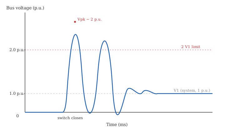
so the energization transient for this installation rings at roughly the sixth-and-a-half harmonic of 60 Hz. Because a discharged bank produces an overshoot approaching , the bus of this installation must be expected to see close to twice its normal peak voltage during an uncontrolled energization, ringing at 387 Hz and decaying over several cycles. Figure 1 illustrates the shape of this response.
As illustrated in Figure 1, the bus voltage begins at the pre-fault steady-state level of one per unit, and at the instant the switch closes it swings upward and overshoots toward a first peak that approaches two per unit before the damped oscillation carries it back down and it converges, over several cycles of the natural frequency, to the new steady-state level. The reader should observe two features that drive the equipment specification: the height of the first peak, which sets the overvoltage duty on arresters and connected loads, and the ringing frequency, which determines whether the transient can excite a resonance elsewhere on the system. The horizontal axis is time in milliseconds and the vertical axis is bus voltage in per unit of the system peak voltage.
3. Back-to-Back Switching Transient
3.1 Inrush from an Adjacent Energized Bank
The more severe switching duty arises when a bank is energized onto a bus that already carries one or more energized capacitor banks. In this back-to-back configuration the newly closed bank is charged not primarily through the relatively large system source inductance, but through the very small inductance of the local loop connecting it to the already-energized adjacent bank. Because that loop inductance is orders of magnitude smaller than the system source inductance, the inrush current is far larger and rings at a much higher frequency than the single-bank case. The energized bank behaves as a charged voltage source discharging into the uncharged bank through the series loop inductance.
The peak inrush current for back-to-back switching is
where is the peak inrush current in amperes, is the voltage across the switch at the instant of closing in volts, is the inductance of the loop between the two banks in henries, and is the series-equivalent capacitance of the two banks. The equivalent capacitance of two banks of capacitance and connected through the switching loop is
and the frequency of the back-to-back inrush is set by that equivalent capacitance and the loop inductance:
where is the inrush frequency in hertz. The physical interpretation is important: the inrush magnitude scales with the square root of the ratio of equivalent capacitance to loop inductance, so a small loop inductance, which is exactly what results from placing two banks close together on the same bus with short bus work, produces the largest and fastest inrush. This is the opposite of the single-bank case, where the large source inductance limits the current, and it is why back-to-back switching, not single-bank energization, usually sets the making-current duty on the switching device.
3.2 Worked Example
Take the 25 kV, 12 Mvar bank of Section 2.3 switching against an identical adjacent bank, with a loop inductance between the two banks of 5 microhenries, a value representative of closely spaced banks connected by a few meters of bus. The equivalent capacitance of the two equal banks is
The voltage across the switch at the worst-case closing instant is the peak line-to-neutral voltage,
Substituting into the inrush expressions gives a peak current of
ringing at a frequency of
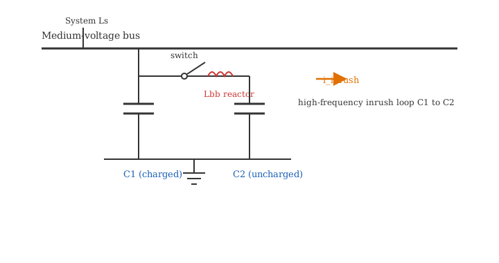
A 46 kA inrush at 14 kHz far exceeds the inrush that any ordinary vacuum or SF6 switching device is rated to make without limitation, and it is precisely the duty that IEEE Std C37.012 requires be evaluated and controlled. Figure 2 shows the circuit that produces this inrush and the location of the current-limiting reactor used to reduce it.
As illustrated in Figure 2, the energized bank C1 discharges through the closing switch and the loop inductance into the uncharged bank C2, and the inrush current circulates in the tight loop formed by the two banks rather than flowing back through the system source. The reader should note the position of the optional series reactor in the switching loop: by deliberately increasing the loop inductance, the reactor directly reduces both the inrush peak, which falls with the square root of the added inductance, and the inrush frequency. The diagram identifies the medium-voltage bus, both banks with their grounded-wye connection, and the current-limiting reactor whose sizing is treated in Section 4.
4. Mitigation Methods and Standard-Referenced Duties
4.1 Series Current-Limiting Reactors
The most direct means of controlling back-to-back inrush is to insert a series reactor in the switching loop, deliberately raising the loop inductance from its stray value to a designed value. Because the inrush peak varies as the inverse square root of the loop inductance, a modest reactor produces a large reduction. Sizing the reactor to a value in the worked example reduces the inrush to
at a frequency of
so a 200 microhenry reactor cuts the inrush from 46 kA at 14 kHz to about 7.3 kA at 2.2 kHz, bringing both the magnitude and the frequency within the range that a standard interrupting device can make and that IEEE Std C37.012 treats as a defined switching duty. The design lever here is the reactor value: the engineer selects it so that the resulting inrush peak is comfortably below the device's rated making current and the frequency is low enough that the reactor and its transient recovery voltage remain within the device's capability.
4.2 Synchronous Closing and Restrike Overvoltage
An alternative to limiting the inrush by impedance is to control the instant of closing so that each pole closes at or near the voltage zero of its phase, minimizing the step in voltage that drives the transient. A synchronous or point-on-wave closing control monitors the system voltage and commands the mechanism so that contact touch occurs within a small window around the zero crossing, which sharply reduces both the energization overshoot and the back-to-back inrush without any added series impedance.
A related concern is restrike, which occurs when the switching device fails to hold off the recovery voltage after interrupting a capacitive current and re-establishes an arc. Because the capacitor retains a trapped charge after interruption, a restrike can superimpose a fresh transient on the already-charged bank, and successive restrikes can escalate the voltage. The bounding overvoltage from a single restrike is
where is the peak voltage that can appear across the bank following a restrike and is the peak recovery voltage across the open device. This three-per-unit bound is the reason IEEE Std C37.012 places such emphasis on the restrike performance of capacitance-current switching devices and classifies them by their restrike probability; a device applied to capacitor switching must be selected for a low restrike class so that the three-per-unit escalation is a remote rather than routine event.
4.3 Pre-Insertion Resistors and Application Limits
A third mitigation method inserts a resistor or inductor into the circuit for a few milliseconds before the main contacts close, damping the energization transient during the interval when the overshoot would otherwise be largest, then shorting it out for continuous operation. Pre-insertion resistors are the classical solution on high-voltage circuit breakers and are highly effective at limiting the single-bank energization overshoot toward 1.1 to 1.3 per unit.
Whichever mitigation is chosen, the application must close against the continuous capability limits of IEEE Std 1036, which permits a capacitor unit to operate continuously at up to 110 percent of rated voltage and to carry up to 135 percent of rated current including the effects of overvoltage, harmonics, and manufacturing tolerance. The transient quantities computed above must be checked against these continuous limits and against the making, breaking, and restrike duties of IEEE Std C37.012 for the switching device. The design is complete only when the energization overshoot, the back-to-back inrush magnitude and frequency, and the restrike overvoltage have each been computed for the specific installation and shown to fall within both standards, with mitigation applied wherever a computed quantity exceeds a limit.
5. Conclusion
The switching of shunt capacitor banks produces two transients that the application engineer must quantify before specifying the bank and its switching device. Single-bank energization excites a series resonance between the system source inductance and the bank capacitance, ringing at a natural frequency of a few hundred hertz and driving the bus voltage toward a peak that approaches two per unit for a discharged bank. Back-to-back switching, by contrast, discharges an energized bank into an adjacent uncharged bank through a small loop inductance, producing an inrush of tens of kiloamperes at several kilohertz that ordinarily sets the making-current duty. The worked 25 kV, 12 Mvar example showed a 387 Hz energization transient approaching two per unit and a 46 kA, 14 kHz back-to-back inrush that a 200 microhenry series reactor reduces to a manageable 7.3 kA at 2.2 kHz. Each of these quantities maps directly to an application limit or test duty in IEEE Std 1036 and IEEE Std C37.012, and the combination of series reactors, synchronous closing, and pre-insertion resistors gives the engineer the means to bring any installation within those limits. The discipline the standards impose is simple to state and essential to follow: compute every transient quantity for the actual installation, compare it to the governing limit, and mitigate wherever the computation exceeds the limit.
References
- IEEE Std 1036-2020, IEEE Guide for the Application of Shunt Power Capacitors, Institute of Electrical and Electronics Engineers, 2020.
- IEEE Std C37.012-2014, IEEE Guide for the Application of Capacitance Current Switching for AC High-Voltage Circuit Breakers Above 1000 V, Institute of Electrical and Electronics Engineers, 2014.
- IEEE Std 18-2012, IEEE Standard for Shunt Power Capacitors, Institute of Electrical and Electronics Engineers, 2012.
- T. J. E. Miller, Reactive Power Control in Electric Systems, John Wiley & Sons, 1982.
- A. Greenwood, Electrical Transients in Power Systems, 2nd ed., John Wiley & Sons, 1991.